If you are asking what micro soldering is, chances are you are dealing with electronics that do not forgive mistakes.
Pads are smaller. Components are tighter. Heat margins are thinner. And one careless second can lift a trace that took weeks to design.
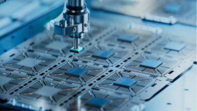
Micro soldering is the precision process of soldering extremely small electronic components and connections, typically under magnification, using specialized tools and controlled heat. It is commonly used in PCB repair, mobile device restoration, fine-pitch IC work, and advanced electronic assembly.
But describing it that way makes it sound simple. It is not.
The Scale Changes Everything
Traditional soldering deals with through-hole components or larger surface-mount devices. There is room for error. There is visible solder flow. There is mechanical forgiveness.
Micro soldering operates in millimeters. Sometimes microns.
We are talking about:
- Fine-pitch integrated circuits
- Micro capacitors and resistors
- Ball Grid Array (BGA) components
- Delicate PCB traces
- High-density interconnect boards
At this scale, heat distribution behaves differently. Surface tension behaves differently. Even the solder alloy selection becomes critical.
One degree too hot, and the pad lifts. One second too long, and the substrate warps. Too little heat, and the joint fails electrically.
Precision is not optional. It is structural.
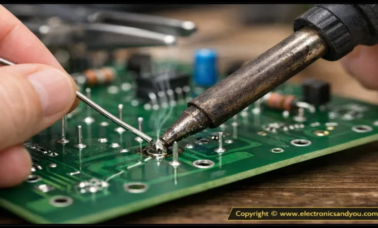
The Core Tools Behind Micro Soldering
Micro soldering is not performed with a basic iron from a hardware store.
It typically requires:
- Temperature-controlled soldering stations
- Micro-tipped soldering irons
- Hot air rework stations
- Stereo microscopes or digital magnification systems
- Precision tweezers and micro tools
- Flux formulated for fine-pitch work
Magnification is essential. Many micro soldering tasks cannot be performed accurately with the naked eye.
Thermal control is equally critical. Advanced stations allow tight temperature calibration because excess heat damages multilayer PCBs internally, not just on the surface.
The board may look intact while inner layers have already separated.
Where Micro Soldering Is Used
Micro soldering appears in environments where component density is extreme and replacement is more practical than full system discard.
Common applications include:
- Smartphone motherboard repair
- Laptop and tablet board-level repair
- Gaming consoles and embedded devices
- Medical electronics servicing
- Aerospace and industrial PCB repair
- Advanced prototype modification
In many cases, replacing an entire board is cost-prohibitive or impossible. Micro soldering allows component-level intervention.
It restores functionality without replacing the architecture.
The Process Behind the Precision
Micro soldering is not simply about attaching metal to metal. It follows controlled steps:
- Diagnosis of the failure at component level
- Surface preparation and flux application
- Controlled heat delivery
- Component placement or removal
- Inspection under magnification
- Electrical continuity testing
In BGA work, reballing may be required. That involves removing microscopic solder balls and replacing them before reinstalling the chip.
Alignment tolerance is tight. Misalignment may not be visible but will cause intermittent failures.
Cleanliness is critical. Flux residue can create leakage paths or corrosion over time.
This is technical work, not improvisation.
Why It Is Harder Than It Looks
Online videos often make micro soldering appear effortless.
Reality is different.
Modern PCBs contain multiple internal copper layers. Excessive heat can cause delamination. Components are often lead-free, requiring higher temperatures. Thermal mass varies across the board, making uniform heating challenging.
And then there is ESD risk.
Electrostatic discharge at microscopic scale can destroy sensitive ICs instantly.
A professional micro soldering setup controls not only temperature but also grounding, airflow, humidity, and tool calibration.
Because failure at this level is silent. The device may power on. It may even function briefly. Then it fails again.
When Micro Soldering Makes Sense
Micro soldering is appropriate when:
- The device has high replacement cost
- Data recovery is critical
- The board is unavailable or discontinued
- Failure is isolated to a small component
- Precision repair is more sustainable than disposal
It is less appropriate when structural board damage is extensive or when multiple subsystems have failed beyond repair.
Context determines viability.
Small Scale, High Stakes
Micro soldering operates at the intersection of material science, heat control, and steady execution.
The components are small. The consequences are not.
When done correctly, it restores full electrical integrity. When done poorly, it introduces hidden instability.
At a microscopic scale, skill is measurable in microns.
And in modern electronics, that margin often determines whether a device returns to service or becomes waste.
FAQs
- Is micro soldering only for phone repairs?
No. While commonly associated with smartphone repair, micro soldering is widely used in laptops, medical devices, industrial electronics, aerospace systems, and prototype development.
- Can micro soldering damage a PCB?
Yes, if performed without proper temperature control and technique. Excessive heat can lift pads, damage internal layers, or weaken surrounding components.
- How do I know if a device can be fixed with micro soldering?
If the failure is isolated to a specific component, trace, or solder joint and the board is structurally intact, micro soldering is often a viable repair method. Severe multilayer damage or widespread electrical failure may require full board replacement.