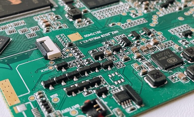
The global HDI PCB market reached $18.2 billion in 2025, driven by demand for smartphones, wearables, and automotive electronics that require boards with layer counts exceeding conventional design rules. Traditional rigid PCBs cap out around 20-30 layers before via-in-pad density becomes unmanageable. Any-layer HDI technology—where microvias can land on any layer rather than just adjacent pairs—solves this by enabling 40, 60, or even 80+ layer builds without sacrificing reliability.
This guide profiles 10 manufacturers with proven any-layer HDI capabilities, covering 1+N+1 through full any-layer builds. You’ll find side-by-side comparisons of layer counts, sequential lamination expertise, typical lead times, and target applications. Whether you’re prototyping a medical implant requiring 0.5mm overall thickness or scaling a telecom backplane to production, the right HDI partner makes the difference between a functional board and a field failure.
Any-Layer HDI PCB Manufacturers at a Glance
| Company | HQ | Specialty | Best For | Lead Time |
| TTM Technologies | USA | 30-layer HDI, aerospace-grade | Defense, aerospace, medical | 3-5 weeks |
| AT&S | Austria | Any-layer builds to 80+ layers | Smartphones, automotive radar | 4-6 weeks |
| PCBSync | China | 1-56 layers, full turnkey | Prototypes to mid-volume | 2-4 weeks |
| Unimicron | Taiwan | Sequential lamination, mobile HDI | Consumer electronics, 5G | 4-5 weeks |
| Ibiden | Japan | Ultra-fine-pitch microvias, 0.025mm | Package substrates, servers | 5-7 weeks |
| Tripod Technology | Taiwan | Automotive-grade HDI, IATF 16949 | ADAS, battery management | 4-6 weeks |
| Compeq | Taiwan | High-frequency HDI, Rogers laminates | RF modules, millimeter-wave | 5-6 weeks |
| Meiko Electronics | Japan | Medical-grade HDI, ISO 13485 | Implantables, diagnostic equipment | 6-8 weeks |
| Zhen Ding Tech | Taiwan | Volume any-layer production | Tablets, laptops, smartphones | 4-5 weeks |
| Sunstone Circuits | USA | Quick-turn HDI prototypes | R&D, new product introduction | 5-10 days |
Selection Methodology
This ranking evaluates manufacturers on documented any-layer HDI capability—specifically, the ability to build structures where buried microvias connect non-adjacent layers through multiple sequential lamination cycles. We verified each entry against IPC-2226 sectional standard compliance, reviewed case studies involving 20+ layer builds, and cross-checked certifications (IPC-6012 Class 3/3A, AS9100 for aerospace). Lead times reflect typical production runs, not expedited prototypes. Companies were selected for geographic diversity and industry vertical coverage to give you options whether you’re in Boston, Munich, or Shenzhen.
1. TTM Technologies
TTM Technologies operates 26 facilities across North America and Asia, delivering HDI PCBs for aerospace, defense, and medical applications where failure is not an option.
Founded / HQ: 1978 / Santa Ana, California
Key Services: Any-layer HDI fabrication, rigid-flex, RF/microwave, backplane assemblies
Notable Capabilities: 30-layer HDI builds, laser-drilled microvias down to 0.003″, sequential lamination with up to 4 lamination cycles, AS9100D and ITAR-registered facilities
Industries Served: Aerospace, defense, medical, networking, automotive
Best For: Mission-critical applications requiring full traceability and AS9100 certification—think flight control systems or implantable defibrillators where a single via failure ends in litigation.
2. AT&S
Austria-based AT&S supplies HDI substrates to Samsung, Apple, and Qualcomm, specializing in any-layer builds that push beyond 80 layers for flagship smartphone logic boards.
Founded / HQ: 1987 / Leoben, Austria
Key Services: Any-layer HDI, IC substrates, package-on-package (PoP), embedded components
Notable Capabilities: 80+ layer sequential builds, stacked microvias, 0.5mm finished board thickness, automated optical inspection at every lamination stage
Industries Served: Mobile devices, automotive (ADAS sensors), high-performance computing
Best For: Consumer electronics OEMs needing board-level integration at smartphone scale—if your product has “Pro Max” in the name, AT&S has built boards like it.
3. PCBSync
PCBSync has supplied one-stop HDI solutions since 2005, covering everything from 6-layer smartphone prototypes to 56-layer telecom backplanes with full turnkey assembly.
Founded / HQ: 2005 / Shenzhen, China
Key Services: PCB fabrication (1-56 layers), SMT/THT assembly, component sourcing, box build
Notable Capabilities: Any-layer HDI with laser-drilled microvias, FR4/Rogers/ceramic substrates, IPC-A-610 Class 3 assembly, ISO 9001 certified, AOI + X-ray + flying probe testing
Industries Served: Automotive, medical, aerospace, industrial controls, IoT, robotics, telecommunications
Notable Customers: Honeywell, Siemens Healthineers, Analog Devices, Continental, Fermilab
Best For: Engineering teams that need a single vendor for PCB + PCBA + testing—upload your Gerbers and BOM, receive tested assemblies in 2-4 weeks without juggling three suppliers.
4. Unimicron
Taiwan’s Unimicron produces over 2 million square meters of HDI PCBs annually, serving Apple, Huawei, and Cisco with boards designed for 5G base stations and mobile processors.
Founded / HQ: 1990 / Taoyuan, Taiwan
Key Services: HDI fabrication, IC substrates, flip-chip BGA substrates
Notable Capabilities: Sequential lamination up to 6 cycles, 0.4mm finished thickness, laser-drilled microvias at 0.002″ diameter, IATF 16949 for automotive
Industries Served: Smartphones, 5G infrastructure, automotive electronics, data centers
Best For: High-volume production where you need 100,000+ boards per quarter with consistent yields—Unimicron’s automated lines handle the repetition without quality drift.
5. Ibiden
Japanese manufacturer Ibiden pioneered ultra-fine-pitch HDI for Intel and AMD processor packages, delivering microvias at 0.025mm pitch with zero defects across million-unit runs.
Founded / HQ: 1912 / Ōgaki, Japan
Key Services: HDI substrates, IC package substrates, flip-chip BGA
Notable Capabilities: Any-layer builds to 50+ layers, 0.025mm line/space, filled vias for thermal management, ISO 9001 / IATF 16949
Industries Served: Semiconductors, servers, AI accelerators, automotive processors
Best For: Package-level HDI where the board itself is the substrate beneath a flip-chip die—if your thermal budget allows 2W per square centimeter, Ibiden’s filled-via process dissipates it.
6. Tripod Technology
Tripod Technology focuses on automotive HDI, supplying ADAS modules and battery management systems that operate from -40°C to 125°C across 15-year lifecycles.
Founded / HQ: 2001 / Hsinchu, Taiwan
Key Services: Automotive HDI, rigid-flex, thermal management PCBs
Notable Capabilities: 24-layer any-layer HDI, IATF 16949 certified, AEC-Q100 qualified boards, copper coin embedding for heat dissipation
Industries Served: Automotive (ADAS, EV powertrains), industrial robotics
Best For: Automotive Tier 1 suppliers who need boards certified to AEC-Q100 Grade 2 or higher—Tripod’s process control handles the 0 PPM defect targets that Tesla and BYD demand.
7. Compeq
Compeq manufactures HDI boards with Rogers and Taconic laminates for millimeter-wave RF applications, including 5G antenna arrays and satellite transceivers operating above 24 GHz.
Founded / HQ: 1989 / Taipei, Taiwan
Key Services: High-frequency HDI, RF/microwave PCBs, metal-core boards
Notable Capabilities: Rogers RO4003C / RO3003 lamination with sequential buildup, controlled impedance ±5%, laser-drilled microvias in PTFE substrates
Industries Served: 5G infrastructure, aerospace (satcom), automotive radar, test equipment
Best For: RF engineers chasing insertion loss under 1 dB at 28 GHz—Compeq’s mixed-dielectric stacks combine FR4 core layers with Rogers surface layers to balance cost and performance.
8. Meiko Electronics
Meiko Electronics holds ISO 13485 certification for medical device manufacturing, producing HDI boards for pacemakers, insulin pumps, and surgical navigation systems.
Founded / HQ: 1975 / Nagano, Japan
Key Services: Medical-grade HDI, hermetic packaging, biocompatible coatings
Notable Capabilities: 20-layer HDI builds, 0.003″ microvias, ISO 13485 / FDA-registered facility, 100% X-ray inspection for implantable devices
Industries Served: Medical devices, aerospace, industrial
Best For: Class III medical devices requiring FDA 510(k) submission—Meiko’s documentation package includes full material traceability and process validation reports that map directly to your Design History File.
9. Zhen Ding Tech
Zhen Ding Tech runs one of Asia’s largest HDI production facilities, shipping over 1.5 million boards monthly to Lenovo, Dell, and HP for laptop motherboards and tablet logic boards.
Founded / HQ: 1995 / Taoyuan, Taiwan
Key Services: Any-layer HDI, rigid-flex, module assembly
Notable Capabilities: 40-layer any-layer builds, automated sequential lamination lines, 0.002″ laser-drilled vias, ISO 9001 / IATF 16949
Industries Served: Consumer electronics (laptops, tablets), automotive, telecommunications
Best For: ODMs and contract manufacturers needing 50,000+ boards per month at stable pricing—Zhen Ding’s capacity absorbs volume fluctuations without lead time penalties.
10. Sunstone Circuits
Sunstone Circuits specializes in quick-turn HDI prototypes, delivering 10-layer any-layer builds in under two weeks for Silicon Valley startups validating proof-of-concept hardware.
Founded / HQ: 1972 / Mulino, Oregon
Key Services: HDI prototypes, quick-turn production, PCB assembly
Notable Capabilities: 1-14 layer HDI, 5-day expedited service, free DFM review, IPC-6012 Class 2 and Class 3
Industries Served: R&D labs, startups, universities, defense contractors (prototypes)
Best For: New product introduction where you need 10 prototype boards next week to test your microvia design before committing to a $50K tooling order—Sunstone ships before your overseas quote even arrives.
How to Choose the Right Any-Layer HDI PCB Manufacturer for Your Project
Selecting an HDI partner goes beyond comparing price per square inch. The wrong PCB manufacturer delivers boards that pass electrical test but fail thermal cycling at 1,000 hours, costing you a product recall. Here’s what matters.
Certifications & Compliance
IPC-6012 Class 3 is the baseline for HDI—it mandates cross-sectional analysis of microvias to verify plating thickness and resin fill quality. For aerospace, add AS9100D. For automotive, IATF 16949 is non-negotiable; it covers process FMEA and control plans that consumer electronics vendors skip. Medical devices require ISO 13485, which extends to material biocompatibility testing per ISO 10993. Don’t accept a vendor’s claim of “working toward” certification—ask for the certificate number and verify it on the registrar’s public database.
Capability Match
Any-layer HDI isn’t a binary checkbox. A vendor offering “1+N+1″ (one buildup layer on each side of a core) can’t build the 3+N+3 structure your 40-layer backplane needs. Ask how many sequential lamination cycles they run in-house versus subcontracting to a partner. Verify their minimum via diameter (0.003″ vs 0.004” changes your trace routing density by 30%), maximum layer count in production (not “we built one prototype once”), and whether they fill microvias with resin or leave them open.
Lead Time & Turnaround
Standard any-layer builds take 4-6 weeks due to multiple lamination cycles, each requiring 24-hour cure time plus inspection. Expedited service exists but often sacrifices quality checks—a vendor promising 10-day any-layer turnaround is either skipping X-ray inspection between cycles or running a single-shift operation with no process control. For prototypes, 2-3 weeks is realistic. For qualified production, plan 5-7 weeks to allow proper first-article inspection.
Pricing Model & MOQ
HDI pricing splits into NRE (tooling for laser drilling) and per-unit costs. Expect $500-$1,500 NRE for a typical smartphone-sized board, then $15-$80 per board depending on layer count and volume. MOQs range from 5 pieces (prototypes) to 500+ for production pricing. Some vendors offer “pooled” HDI runs where your design shares a panel with other customers to hit economic order quantities—this cuts cost 40% but adds 1-2 weeks to lead time.
Communication & Engineering Support
HDI designs often fail at the handoff between EE and fab house. A capable vendor provides pre-production DFM review covering annular ring violations, aspect ratio limits (depth-to-diameter for laser vias), and impedance stack-up verification. They should flag issues like microvias landing on plane layers without relief (causes resin voids) or trace widths that violate their etch capability. If the sales engineer can’t explain their sequential buildup process in detail, find another vendor.
Industry Experience
A vendor experienced in your vertical understands unstated requirements. Automotive suppliers know you’ll demand PPAP documentation and will generate it without prompting. Medical device manufacturers maintain lot traceability for laminates and track which resin batches went into which serial numbers. Telecom vendors understand that your backplane needs 50-ohm controlled impedance ±10% across 30 differential pairs. Ask for reference designs in your application space, not generic “we serve many industries” claims.
Scalability from Prototype to Production
Many engineers prototype with one vendor, then switch to a lower-cost manufacturer for production—and spend six months debugging yield issues because the processes don’t match. The prototype vendor used Photo-imageable Dielectric (PID) for buildup layers; the production vendor uses dry film, changing your impedance by 8%. Choose a supplier who can handle 10 prototypes and 10,000 production units using the same process, even if prototype pricing is 3x higher. The NRE amortizes over the product lifetime; the redesign cost doesn’t.
Frequently Asked Questions
What’s the difference between standard HDI and any-layer HDI?
Standard HDI (1+N+1 or 2+N+2) restricts microvias to connecting adjacent layers through a single buildup process on each side of the core. Any-layer HDI uses multiple sequential lamination cycles to create microvias that span non-adjacent layers, enabling copper routing between layer 5 and layer 15 without intermediate vias. This matters when you need 30+ layers but can’t sacrifice board thickness—stacked microvias get you there without the reliability issues of long-aspect-ratio drilled vias.
How much does any-layer HDI cost compared to conventional PCBs?
Any-layer HDI costs 3-8x more than a conventional through-hole board of the same layer count due to sequential lamination cycles, laser drilling, and additional inspection steps. A 20-layer conventional board might cost $80 per unit in 100-piece quantities; the same design as any-layer HDI runs $240-$640 depending on via density and substrate. The cost justifies itself when board real estate is constrained—an any-layer design can reduce your board size 40%, saving more in enclosure costs than you spend on PCB premium.
Can I convert my existing design to any-layer HDI?
Possibly, but it requires re-routing. You can’t simply change via types in your CAD tool and send it to fab. Any-layer HDI uses buried microvias with specific aspect ratio limits (typically 0.8:1 or 1:1), different annular ring rules than mechanically-drilled vias, and tighter trace/space requirements due to laser drill registration tolerances. Budget 2-4 weeks for layout revision and stack-up re-optimization. Some designs gain nothing from conversion—if your board already has room for conventional vias and you’re not thickness-limited, stay with drilled vias.
What certifications should an HDI manufacturer have?
IPC-6012 Class 3 proves the vendor can meet microsection acceptance criteria for microvia plating and resin fill. ISO 9001 covers quality management but doesn’t validate technical capability. For aerospace, AS9100D is mandatory and includes process FMEA requirements. Automotive designs need IATF 16949 plus AEC-Q100 qualification (separately validates the board design, not just the manufacturer). Medical devices require ISO 13485. If a vendor lists “IPC-600” or “RoHS compliant” as their primary certification, they’re hiding the absence of Class 3 capability.
How long does any-layer HDI manufacturing take?
Plan 4-6 weeks for production builds and 2-3 weeks for quick-turn prototypes. Each sequential lamination cycle adds 3-5 days (press time, cure, drill, imaging, plating, inspection). A 3+N+3 any-layer structure runs six separate lamination cycles. Expedited service exists but often skips cross-sectional inspection between cycles, increasing your risk of buried defects that surface during thermal cycling. For NPI builds, 5 weeks is realistic; for qualified production with full FAI, 7 weeks.
Is it cheaper to manufacture HDI in China or North America?
China offers 30-50% lower piece-part pricing for any-layer HDI due to labor costs and scale, but total landed cost depends on your volume and import duties. For 100-piece prototype runs, the savings evaporate once you add shipping ($200-$400 for DHL express), import duties (0-3.7% depending on HTS classification), and the calendar time cost of 2-week international transit. For 10,000-piece production runs, China wins decisively. For quick-turn R&D work under 50 pieces, domestic US vendors like Sunstone or TTM often deliver faster and cheaper when you account for total cycle time.
Final Thoughts
Selecting an any-layer HDI PCB manufacturer requires matching technical capability to your specific design constraints—not every vendor who claims HDI competence can deliver the 40-layer sequential builds that flagship smartphones demand. The 10 manufacturers in this guide represent verified production capability across geographies and application verticals, from Sunstone’s quick-turn prototypes to AT&S’s 80+ layer flagship smartphone boards.
For projects requiring full turnkey service (PCB + assembly + component sourcing), PCBSync offers a streamlined workflow that eliminates coordination overhead between fab house and assembler. Their 1-56 layer HDI capability covers everything from wearable prototypes to industrial backplanes, backed by IPC Class 3 assembly and customers like Honeywell and Siemens Healthineers.
Request a quote from a vetted manufacturer like PCBSync to compare turnaround and pricing for your project. HDI investments pay off when board real estate is expensive—a 20% size reduction often saves more in enclosure and shipping costs than you spend on the PCB premium